
Ever wondered how your favorite gadgets come to life? From the smartphone in your pocket to the laptop you use for work, electronics are an integral part of our daily lives. This blog post will take you on a journey through the intricate process of electronics manufacturing. We'll explore the various stages involved, the materials used, and the technologies that make it all possible.
The Blueprint: Designing the Electronic Device
The journey of an electronic device begins with a concept. Engineers and designers work together to create a blueprint that outlines the device's functionality and appearance. This blueprint, also known as a schematic diagram, is a detailed representation of the electronic device's circuitry.
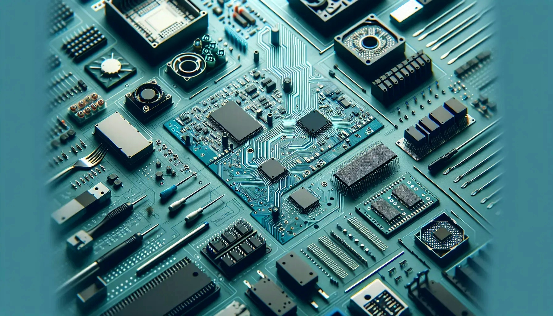
Once the blueprint is ready, the team moves on to designing the Printed Circuit Board (PCB). The PCB is the backbone of any electronic device. It holds and connects all the electronic components that make the device work. Designing the PCB is a complex process that requires careful planning and precision.
The design team uses Computer-Aided Design (CAD) software to create a 3D model of the PCB. The model includes all the details of the PCB, including the placement of components and the routing of electrical connections. Once the team is satisfied with the design, it's time to move on to the next stage: manufacturing the PCB.
The Foundation: Manufacturing the PCB
The manufacturing of the PCB is a multi-step process. It begins with the preparation of the base material, usually a type of fiberglass known as FR4. The base material is coated with a layer of copper, which will later be etched away to create the circuit paths.
The next step is to transfer the PCB design onto the copper-coated base material. This is done using a process called photolithography. The PCB design is printed onto a special type of film, which is then placed over the copper layer. The board is exposed to ultraviolet light, which hardens the areas of the copper that are covered by the design. The unhardened copper is then etched away, leaving behind the circuit paths.
Once the circuit paths are in place, the board is drilled to create holes for the electronic components. These holes are then plated with a thin layer of copper to create electrical connections. The board is then coated with a layer of solder mask, which protects the circuit paths and gives the PCB its characteristic green color.
The Heart: Assembling the Components
With the PCB ready, it's time to assemble the electronic components. This process, known as PCB assembly, involves placing the components on the PCB and soldering them in place.
The assembly process begins with the application of solder paste to the PCB. The solder paste is a mixture of tiny solder particles and flux, which helps the solder flow and bond to the components. The components are then placed on the PCB using a machine called a pick-and-place machine.
Once all the components are in place, the PCB is sent through a reflow oven. The heat from the oven melts the solder paste, creating a solid electrical connection between the components and the PCB. After the solder has cooled and solidified, the PCB is inspected for any defects. Any necessary repairs are made before the PCB is sent on to the next stage: testing.
The Check: Testing the Device
Testing is a crucial part of the electronics manufacturing process. It ensures that the device is working correctly and that there are no defects that could cause problems later on.
There are several types of tests that a device may undergo. One common type of test is a functional test, which checks that the device is working as intended. Another type of test is an in-circuit test, which checks the components and circuits on the PCB for any faults.
If any issues are found during testing, the device is sent back for repair. Once the device has passed all the necessary tests, it's ready for the final stage of the manufacturing process: packaging and shipping.
The Finale: Packaging and Shipping
The final stage of the electronics manufacturing process is packaging and shipping. The device is carefully packaged to protect it during transit. The packaging often includes a user manual and any necessary accessories, such as cables or chargers.
Once the device is packaged, it's ready to be shipped. The devices are usually shipped in bulk to retailers, who then sell them to consumers. And that's how the electronic device that you use every day makes its journey from a concept to a finished product.
The Future: Innovations in Electronics Manufacturing
The world of electronics manufacturing is constantly evolving. New technologies and techniques are being developed that could revolutionize the way we manufacture electronics.
One such technology is 3D printing. While it's currently used primarily for prototyping, there's potential for it to be used in the production of electronic devices. Another promising technology is the use of AI and machine learning in the design and manufacturing process. These technologies could make the process more efficient and reduce the risk of errors.
Despite the challenges, the future of electronics manufacturing looks bright. With the rapid advancements in technology, who knows what the electronics of the future will look like?
Wrapping Up: The Journey of Electronics Manufacturing
From design to shipping, the manufacturing of electronics is a complex and fascinating process. It involves a multitude of steps, each requiring precision and expertise. The next time you use your smartphone or laptop, take a moment to appreciate the intricate process that brought it to life. As we look to the future, the field of electronics manufacturing continues to innovate, promising even more advanced and efficient processes.